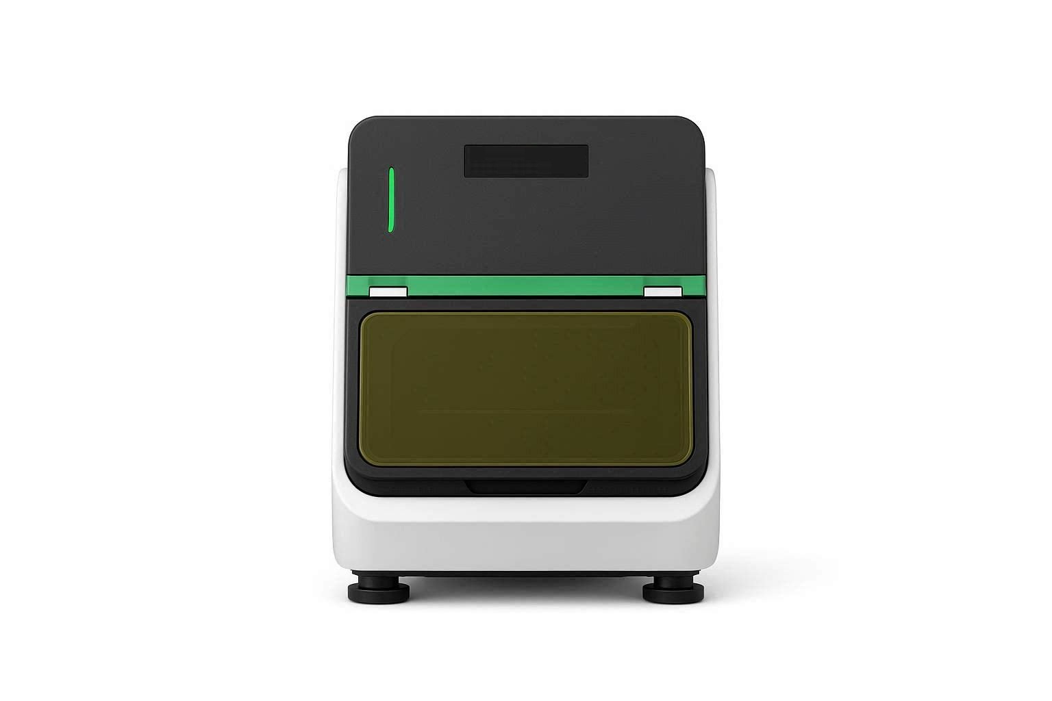
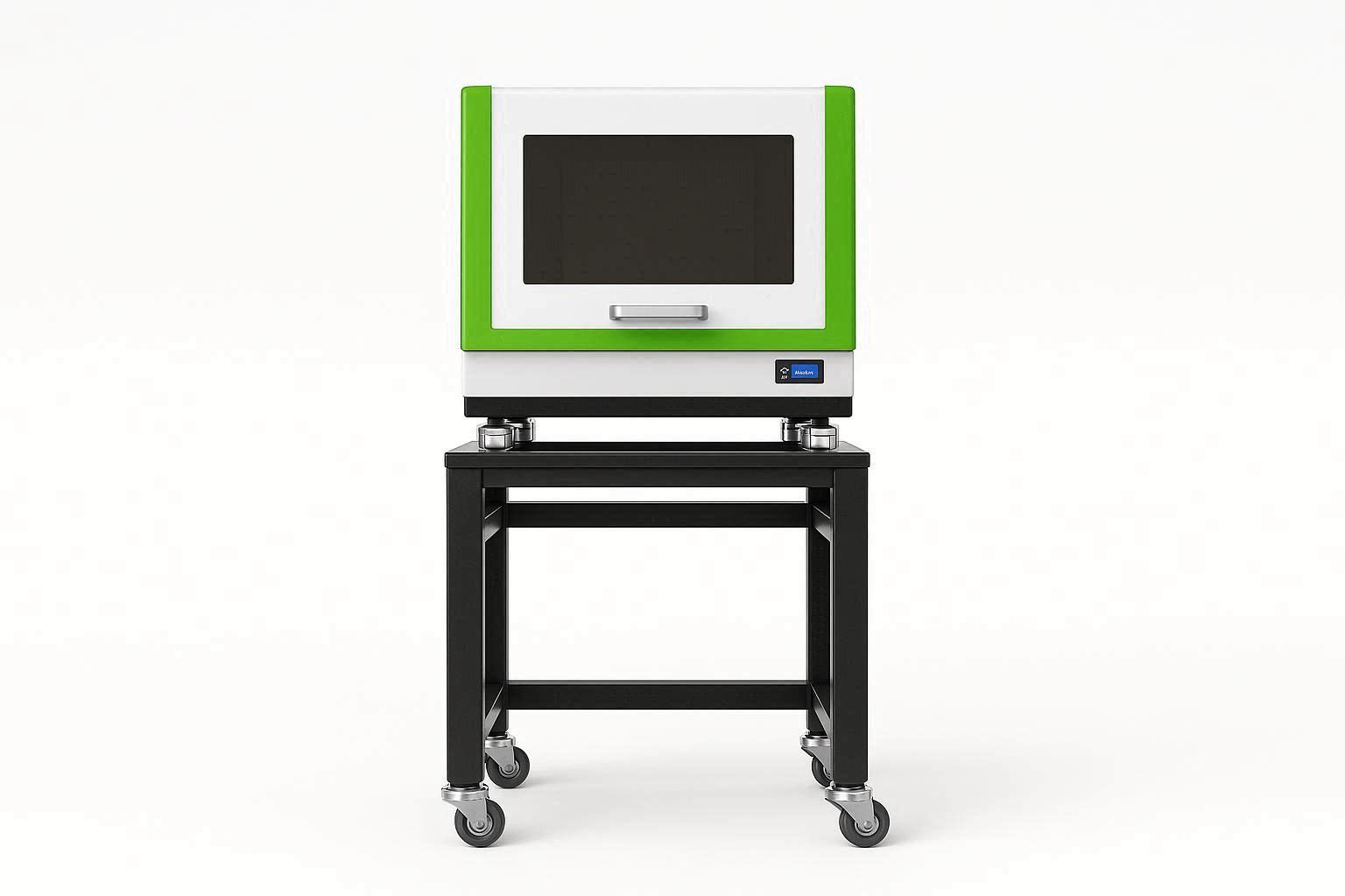
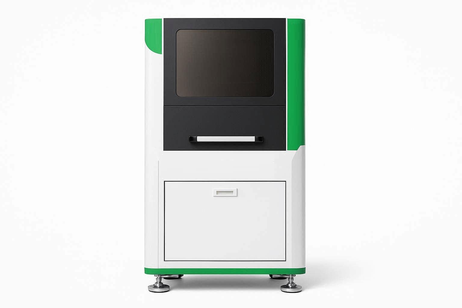
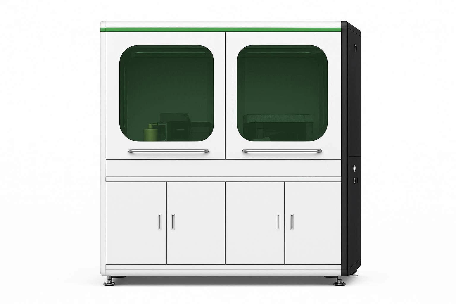
Maskless Lithography Machines
Description

Maskless Lithography Machine is cutting-edge tool revolutionizing the semiconductor and microfabrication industries. Unlike traditional lithography that relies on masks, maskless lithography systems directly write intricate patterns onto substrates using focused electron, laser, or ion beams. This innovative technology offers unparalleled flexibility, speed, and cost savings, making it ideal for small-scale production, rapid prototyping, and custom device fabrication.
Key Benefits of Maskless Lithography Machines:
- Eliminates Mask Costs and Lead Times: Direct writing reduces manufacturing costs and accelerates production cycles.
- High-Resolution Patterning: Enables the creation of nanometer-scale features for advanced semiconductor devices.
- Versatile Applications: Perfect for microchips, sensors, MEMS, biomedical devices, and research prototypes.
- Flexible and Scalable: Available in desktop research units or large industrial systems for high-volume manufacturing.
Applications of Maskless Lithography Machines:
- Microchips and integrated circuits
- Sensors and MEMS devices
- Biomedical and research devices
- Advanced prototyping for new materials and structures
System Variations:
- Desktop or benchtop units for research and development
- Large-scale industrial systems for commercial production
Advantages Maskless Lithography Machine:
- Higher resolution and precision
- Faster iteration cycles
- Greater design flexibility
- Reduced costs, especially for low-volume production
Why Choose Maskless Lithography?
As technology advances, maskless lithography offers higher resolution, faster processing speeds, and greater design flexibility. It is a game-changer for industries demanding rapid innovation and customization. Whether for small-batch production or cutting-edge research, maskless lithography machines are essential tools for modern manufacturing.
Discover the Future of Patterning Technology with Maskless Lithography Machines — the ideal solution for high-precision, cost-effective, and flexible device fabrication.
*For more information, please contact us.
| Parameter | Typical Range of Values | Description / Significance |
| Minimum Feature Size (CD) | 0.3 μm – 5.0μm | The smallest line/space the system can resolve. |
| Overlay / Alignment Accuracy | 0.2μm - 1.0μm | Precision of aligning a new layer to an existing one. |
| Light Source Wavelength | 365, 375, 385, 405 nm | Matches the absorption spectrum of standard photoresists. |
| Write Speed (Throughput) | 20 mm2/min - 5000 + mm2/min | Critical for scaling from research to mass production. |
| Substrate Size (Travel) | 5 x 5mm to 300 x 300mm | Ranges from small chips to 12-inch wafers or PCB panels. |
| Depth of Focus (DOF) | ±1μm− ±20μm | The vertical tolerance for maintaining a sharp image. |
| Address Grid (Step Size) | 10 nm- 100 nm | The smallest increment for digital pattern positioning. |
| Grayscale Levels | 2-1024 levels | Used for 3D micro-structuring (e.g., microlenses). |
| Numerical Aperture (NA) | 0.1-0.9 | Determines the light-gathering power and resolution limit. |
Order Form
About Semiconductor Electronics
SEMI EL project is a global supplier of materials, equipment, spare parts and supplies for the semiconductor industry.
Get In Touch
Email: info@semi-el.com