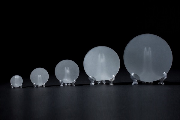
Gallium Antimonide GaSb Wafers
Gallium Antimonide GaSb Wafers
Description

GaAs wafers are grown by VGF (Vertical Gradient Freeze) method and are used for laser diode, LED and microwave semiconductors (MMIC, HBT, HEMT) applications. The substrates are supplied epi-polished and packaged in inert gas packing. Semi-insulating high resistance GaAs substrates are used for IR detectors, gamma photon detectors etc. We provide GaAs substrates 2-6 inch in diameter. Custom sizes and shapes are also available.
Gallium Antimonide (GaSb) wafers are a type of semiconductor material used in the production of electronic and optoelectronic devices that require high-speed and low-power operation. GaSb is a narrow-bandgap semiconductor material, which means that it has a smaller bandgap than conventional semiconductors such as silicon.
GaSb wafers are typically produced using the molecular beam epitaxy (MBE) or metal-organic chemical vapor deposition (MOCVD) methods. In the MBE method, a substrate made of GaSb is heated in a vacuum chamber and a source material, typically gallium and antimony, is heated until it vaporizes. The vapor is transported by a carrier gas, typically hydrogen, and deposited on the GaSb substrate, forming a single crystal GaSb layer. In the MOCVD method, a GaSb layer is deposited on a substrate by reacting a gas mixture containing gallium and antimony precursors at high temperatures.
Once the GaSb crystal is grown, it is sliced into thin wafers and polished to a high degree of flatness and smoothness. The resulting GaSb wafers can then be used as a platform for the growth of additional semiconductor layers, which can be doped with impurities to create p-type and n-type regions for device fabrication.
GaSb wafers have several advantages over other semiconductor materials such as silicon. GaSb has a higher electron mobility and a higher electron saturation velocity than silicon, which makes it suitable for high-speed electronic devices. Additionally, GaSb has a lower thermal conductivity and a lower thermal expansion coefficient than silicon, which makes it suitable for applications such as thermophotovoltaic devices and infrared detectors.
| Item | Specifications | ||
| Dopant | Undoped | Zinc | Tellurium |
| Conduction Type | P-type | P-type | N-type |
| Wafer Diameter | 2″ | ||
| Wafer Orientation | (100)±0.5° | ||
| Wafer Thickness | 500±25um | ||
| Primary Flat Length | 16±2mm | ||
| Secondary Flat Length | 8±1mm | ||
| Carrier Concentration | (1-2)x1017cm-3 | (5-100)x1017cm-3 | (1-20)x1017cm-3 |
| Mobility | 600-700cm2/V.s | 200-500cm2/V.s | 2000-3500cm2/V.s |
| EPD | <2×103cm-2 | ||
| TTV | <10um | ||
| BOW | <10um | ||
| WARP | <12um | ||
| Laser Marking | upon request | ||
| Suface Finish | P/E, P/P | ||
| Epi Ready | yes | ||
| Package | Single wafer container or cassette | ||
| Item | Specifications | ||
| Conduction Type | P-type | P-type | N-type |
| Dopant | Undoped | Zinc | Tellurium |
| Wafer Diameter | 3″ | ||
| Wafer Orientation | (100)±0.5° | ||
| Wafer Thickness | 600±25um | ||
| Primary Flat Length | 22±2mm | ||
| Secondary Flat Length | 11±1mm | ||
| Carrier Concentration | (1-2)x1017cm-3 | (5-100)x1017cm-3 | (1-20)x1017cm-3 |
| Mobility | 600-700cm2/V.s | 200-500cm2/V.s | 2000-3500cm2/V.s |
| EPD | <2×103cm-2 | ||
| TTV | <12um | ||
| BOW | <12um | ||
| WARP | <15um | ||
| Laser marking | upon request | ||
| Suface finish | P/E, P/P | ||
| Epi ready | yes | ||
| Package | Single wafer container or cassette | ||
| Item | Specifications | ||
| Conduction Type | P-type | P-type | N-type |
| Dopant | Undoped | Zinc | Tellurium |
| Wafer Diameter | 4″ | ||
| Wafer Orientation | (100)±0.5° | ||
| Wafer Thickness | 800±25um | ||
| Primary Flat Length | 32±2mm | ||
| Secondary Flat Length | 18±1mm | ||
| Carrier Concentration | (1-2)x1017cm-3 | (5-100)x1017cm-3 | (1-20)x1017cm-3 |
| Mobility | 600-700cm2/V.s | 200-500cm2/V.s | 2000-3500cm2/V.s |
| EPD | <2×103cm-2 | ||
| TTV | <12um | ||
| BOW | <12um | ||
| WARP | <15um | ||
| Laser marking | upon request | ||
| Suface finish | P/E, P/P | ||
| Epi ready | yes | ||
| Package | Single wafer container or cassette | ||
Order Form
About Semiconductor Electronics
SEMI EL project is a global supplier of materials, equipment, spare parts and supplies for the semiconductor industry.
Get In Touch
Email: info@semi-el.com

